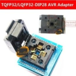
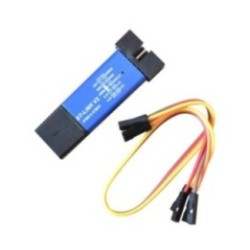
J-Link BASE is a USB powered JTAG debug probe supporting a large number of CPU cores. Based on a 32-bit RISC CPU, it can communicate at high speed with the supported target CPUs. J-Link is used around the world in tens of thousand places for development and production (flash programming) purposes.
 Security policy
(edit with the Customer Reassurance module)
 Delivery policy
(edit with the Customer Reassurance module)
 Return policy
(edit with the Customer Reassurance module)
J-Link BASE is a USB powered JTAG debug probe supporting a large number of CPU cores. Based on a 32-bit RISC CPU, it can communicate at high speed with the supported target CPUs. J-Link is used around the world in tens of thousand places for development and production (flash programming) purposes.


The J-Link debug probes are supported by all major IDEs including Eclipse, GDB-based IDEs and SEGGER Embedded Studio.
Including all models, more than 500,000 J-Links have been shipped so far, making J-Link probably the most popular debug probe for ARM cores and the de-facto standard.


Specifications:
Supported OS 	Microsoft Windows 2000, XP, 2003, Vista, 7 and newer (32 bit and 64 bit versions)
Linux
Mac OSX 10.5 and higher
Electromagnetic compatibility (EMC) 	EN 55022, EN 55024
Operating temperature 	+5°C ... +60°C
Storage temperature 	-20°C ... +65 °C
Relative humidity (non-condensing) 	Max. 90% rH
Mechanical
Size (without cables) 	100mm x 53mm x 27mm
Weight (without cables) 	70g
Size compact device (without cables) 	47mm x 40mm x 14mm
Weight compact device (without cables) 	20g
Available Interfaces
USB interface 	USB 2.0 (High-Speed)
Target interface 	JTAG/SWD 20-pin
JTAG/SWD Interface, Electrical
Power supply 	USB powered
Max. 50mA + Target Supply current.
Target interface voltage (VIF) 	1.2V ... 5V
Current drawn from target voltage sense pin (VTRef) 	< 25µA
Target supply voltage 	5V (derived from USB voltage)
Target supply current 	Max. 300mA
Reset type 	Open drain. Can be pulled low or tristated
Reset low level output voltage 	VOL <= 10% of VIF
For the whole target voltage range (1.2V <= VIF <= 5V)
LOW level input voltage (VIL) 	VIL <= 40% of VIF
HIGH level input voltage (VIH) 	VIH >= 60% of VIF
For 1.2V >= VIF <= 3.6V
LOW level output voltage (VOL) with a load of 10 kOhm 	VOL <= 10% of VIF
HIGH level output voltage (VOH) with a load of 10 kOhm 	VOH >= 90% of VIF
For 3.6 <= VIF <= 5V
LOW level output voltage (VOL) with a load of 10 kOhm 	VOL <= 20% of VIF
HIGH level output voltage (VOH) with a load of 10 kOhm 	VOH >= 80% of VIF
JTAG/SWD Interface, Timing
Target interface speed 	Max. 15 MHz
SWO sampling frequency 	Max. 30 MHz
Data input rise time (Trdi) 	Trdi <= 20ns
Data input fall time (Tfdi) 	Tfdi <= 20ns
Data output rise time (Trdo) 	Trdo <= 10ns
Data output fall time (Tfdo) 	Tfdo <= 10ns
Clock rise time (Trc) 	Trc <= 3ns
Clock fall time (Tfc) 	Trc <= 3ns
For More Details on PC Click here

For More Details on Portables Click here.
J-Link BASE is a USB powered JTAG debug probe supporting a large number of CPU cores. Based on a 32-bit RISC CPU, it can communicate at high speed with the supported target CPUs. J-Link is used around the world in tens of thousand places for development and production (flash programming) purposes.